
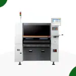
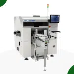
 Pick and Place
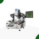 Rework Station
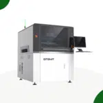 Solder Paste Printers
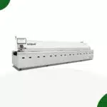 Reflow Ovens
 Reel Storage System
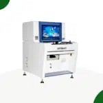 AOI & SPI INSPECTION
 Soldering Machines
 Insertion Machine
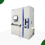
 X-ray inspection
 PCB Handeling
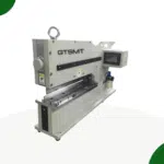 Depaneling Machine
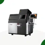
GTSMT X-ray Inspection Systems: Revolutionizing PCB Quality Control

Introduction:
In today’s high-density PCB manufacturing, X-ray inspection has become an indispensable quality assurance tool. GTSMT X-ray inspection systems set new industry standards for defect detection, offering unparalleled precision in identifying hidden solder joint issues and component defects that traditional AOI systems cannot detect.

Key Features of GTSMT X-ray Inspection Systems:
- High-Resolution Imaging Technology
- 130kV/160kV micro-focus X-ray tube options
- Sub-micron resolution (down to 0.5μm)
- Real-time digital imaging with 16-bit grayscale
- Advanced Inspection Capabilities
- Automatic void percentage calculation for BGA/CSP/QFN
- 3D CT scanning option for multilayer PCB inspection
- AI-powered defect recognition algorithms
- User-Friendly Operation
- Intuitive software interface with one-click inspection
- Pre-programmed inspection recipes for common components
- Automatic measurement and reporting functions
- Robust Safety Features
- Lead-shielded cabinet with <1μSv/hr leakage
- Dual safety interlock system
- Emergency stop mechanism
Technical Specifications:
- Maximum sample size: 510×510mm (customizable)
- Geometric magnification: 10-3000X
- Tube voltage: 20-130kV (adjustable)
- Detector resolution: 2048×2048 pixels
- Throughput: up to 300 inspections/hour
Industry Applications:
- Automotive electronics (ADAS, ECU)
- Aerospace and defense PCBs
- Medical device electronics
- High-density consumer electronics
- Semiconductor packaging
Why GTSMT X-ray Systems Outperform Competitors:
- Superior Detection Accuracy
- Identifies defects as small as 0.5μm
- Detects voids, cracks, and insufficient solder with 99.9% reliability
- Unmatched Throughput
- Fastest image processing in the industry
- Parallel inspection of multiple components
- Future-Proof Technology
- Upgradeable software platform
- Compatible with all emerging package types
- Lowest Cost of Ownership
- Minimal maintenance requirements
- Energy-efficient operation
Case Study:
A leading semiconductor manufacturer achieved:
- 98% reduction in field failures
- 40% improvement in first-pass yield
- 30% reduction in inspection time
after implementing GTSMT’s X-ray inspection solution.
Conclusion:
GTSMT X-ray inspection systems represent the gold standard in PCB quality control, combining cutting-edge imaging technology with intelligent analysis capabilities. For manufacturers requiring absolute confidence in their PCB assemblies, GTSMT delivers the most advanced, reliable, and efficient X-ray inspection solutions available today.
For a demonstration of how GTSMT X-ray systems can transform your quality control process, contact our inspection technology experts now.